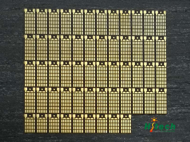
Classifications of Ceramic PCB (Business Opportunities - Marketing & Sales)
Hot-Web-Ads > Business Opportunities > Marketing & Sales
Item ID 15901276 in Category: Business Opportunities - Marketing & Sales
Classifications of Ceramic PCB | |
In accordance with ceramic PCB fabrication methods, they can be classified into three categories: high-temperature co-fired ceramic PCB, low-temperature co-fired ceramic PCB and thick film ceramic PCB. • High-Temperature Co-fired Ceramic (HTCC) PCB As a traditional manufacturing method, high-temperature co-firing is achieved through mixing aluminum oxide and adhesive, plasticizer, lubricant and solvent, leading to raw ceramics by roll forming and curtain coating and implementing circuit tracing on refractory metals like tungsten and molybdenum. Then, it will enter high-temperature oven under 1600°C to 1700°C temperature and carry out baking for 32 to 48 hours after cutting and lamination. To stop tungsten and molybdenum from being oxidized in high temperature, baking should be done in reducing gas such as hydrogen or mixed gas. Ceramic PCBs manufactured by high-temperature co-firing can be applied on small-scale boards, derived boards or carrier circuits. When it comes to large-scale boards, however, high-temperature co-fired ceramic PCBs are challenged due to their unsuitable shrinking tolerance, warpage and relatively high tracing resistance of refractory metals. • Low-Temperature Co-fired Ceramic (LTCC) PCB Low-temperature co-fired ceramic PCB is fabricated by mixing crystal glass, glass composite and non-glass with adhesive with sheet generated and circuit tracing will be implemented by gold paste with high conductivity. After being cut and accurately being formed, it will be placed into oxidizing gas oven at a temperature of 900°C for baking. Low-temperature co-fired ceramic PCB provides a pathway to precious metal paste for circuit tracing and PCB baking can be completed as long as slight improvement is made to thick film baking. Product precision and shrinking tolerance can be improved as well and further optimizations need to be implemented on mechanical intensity and thermal conductivity. • Thick Film Ceramic PCB Thick film gold paste and dielectric paste is repeatedly and alternately printed on ceramic base and goes through baking at a temperature below 1000°C. Although this type of fabrication technology is optimal to large-scale ceramic PCB manufacturing and features relatively high assembly base number, its application is limited due to high cost of gold that also stops solder paste from precipitation. As a result, multi-layer thick film copper circuit technology is developed, which is the most noticeable and popular ceramic PCBs. To prohibit copper from being oxidized, this type of ceramic PCB has to be baked in nitrogen gas, which is the key point of this technology. Furthermore, dielectric paste is generated in nitrogen gas depending on complex multi-layer interconnection structures, which is also a core technology.  | |
| Target State: All States Target City : All Cities Last Update : Jan 20, 2025 10:08 PM Number of Views: 25 | Item Owner : Alisa Contact Email: Contact Phone: (None) |
| Friendly reminder: Click here to read some tips. | |
Hot-Web-Ads > Business Opportunities > Marketing & Sales
© 2025 Hot-Web-Ads.com
USNetAds.com | GetJob.us | CANetAds.com | UKAdsList.com | AUNetAds.com | INNetAds.com | CNNetAds.com | USAOnlineClassifieds.com
2025-02-22 (0.222 sec)