Heavy Copper PCB Design Guidelines (Business Opportunities - Marketing & Sales)
Hot-Web-Ads > Business Opportunities > Marketing & Sales
Item ID 15970053 in Category: Business Opportunities - Marketing & Sales
Heavy Copper PCB Design Guidelines | |
Below are some key design considerations for heavy copper PCBs: Layer Stacking Position thick copper layers close to the board center to minimize warpage. Do not place outer layers next to each other as it exacerbates registration issues. Rotate fiber weave direction 90° between adjacent dielectric layers for stability. Component Placement Ensure sufficient clearance from plane layers for soldermask coverage. Account for component shadows falling on inner copper layers. Check for exposed copper at drilled holes. Thermal Management Place heat generating components over thick copper layers to act as heat spreaders. Provide multiple vias beneath hot components to transfer heat to inner planes. High Current Traces Use copper pouring/polygons for high current lines instead of routing multiple parallel traces. Place adjacent to plated thru-hole vias for heat dissipation. Filled Vias Limit use of filled vias as they impair heat transfer compared to hollow vias. Countersink filled vias and keep soldermask clear of holes. Panel and Tooling Allow generous tolerances for fabrication and assembly. Account for material shrinkage, stretching, and warpage. Use fiducials and test coupons on panel for easy tooling. DFM Analysis Seek DFM feedback from fabricator during design phase. Check manufacturability, especially around heavy copper tolerance issues. Early engagement with the PCB manufacturer smooths the design process and avoids issues during prototyping. 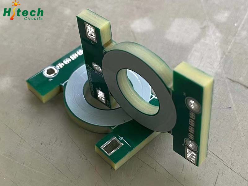 | |
| Target State: All States Target City : All Cities Last Update : Mar 25, 2025 3:39 AM Number of Views: 33 | Item Owner : Alisa Contact Email: Contact Phone: +86 18126460264 |
| Friendly reminder: Click here to read some tips. | |
Hot-Web-Ads > Business Opportunities > Marketing & Sales
© 2025 Hot-Web-Ads.com
USNetAds.com | GetJob.us | CANetAds.com | UKAdsList.com | AUNetAds.com | INNetAds.com | CNNetAds.com | USAOnlineClassifieds.com
2025-03-29 (0.223 sec)