How to make thick copper PCB? (Business Opportunities - Marketing & Sales)
Hot-Web-Ads > Business Opportunities > Marketing & Sales
Item ID 15970238 in Category: Business Opportunities - Marketing & Sales
How to make thick copper PCB? | |
No matter what manufacturing process a PCB manufacturer adopts, there is one technical difficulty that needs to be faced: solving the problem of uneven thickness of heavy copper PCBs. The manufacturing steps and precautions are as follows: Use etching to make inner layer traces on each layer of inner core material of the thick copper PCB (note: open a copper-free area at the same position for each layer of inner core material of the thick copper PCB). Reasonably design the pad position. Lay all inner and outer layers together. Do the corresponding electroplating, surface treatment and conformal coating for the surface of the circuit board. Place an annular ring next to the open area of the core material. All pads are planned to be the same shape and size (shapes include: oval, circle, square and diamond). The spacing between the pads is uniform. The bottom pad position is the same as the top pad position. The way of burying copper in the manufacturing process is also different, and the circuit board manufacturer will choose the appropriate method according to the design of the thick copper PCB. Common heavy copper PCB processes are as follows: Blue Bar: Insert the thick copper bar into the circuit board. This approach reduces the overall weight of the PCB by saving material. The uniformity of the plane is improved by the resin flowing into the space in the copper circuit. Laminate deposition: This process uses a thick base copper. This method is relatively consistent and reliable when placing etch. It is convenient to regulate the edge of the trace and provide fine trace and space. Buried Copper: Insert thick copper into the prepreg in advance. The copper thickness of this method is determined by the resin thickness, using laser cutting. With the advancement of JHD plating technology, our thick copper plated holes and sidewall copper thickness control have become more and more handy. As a result, impedance control and high-current circuits are integrated to achieve a high-density and more stable circuit structure. We will do custom heavy copper pcb production work according to your project needs. It is now possible to mix standard circuits with thick copper on a single board to achieve: reduced layer count, area savings, low impedance power distribution and cost savings. Designers need to discuss manufacturing tolerances based on schematics and PCB design drawings to meet project requirements before performing hybrid articulation. 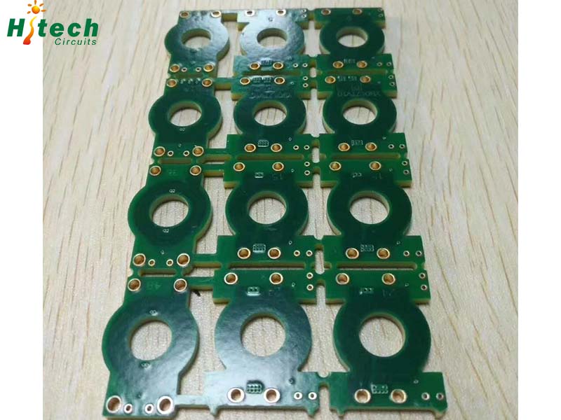 | |
| Target State: All States Target City : All Cities Last Update : Mar 25, 2025 5:18 AM Number of Views: 35 | Item Owner : Alisa Contact Email: Contact Phone: +86 18126460264 |
| Friendly reminder: Click here to read some tips. | |
Hot-Web-Ads > Business Opportunities > Marketing & Sales
© 2025 Hot-Web-Ads.com
USNetAds.com | GetJob.us | CANetAds.com | UKAdsList.com | AUNetAds.com | INNetAds.com | CNNetAds.com | USAOnlineClassifieds.com
2025-03-29 (0.223 sec)